Grating couplers#
Grating couplers are simply components of a photonic circuit that use diffraction to couple light into or out of a waveguide. By utilizing geometry and diffraction, fiber optic cables can be coupled to silicon chips at any location on the chip, instead of just the edges.
How does it work?#
Key to the design of grating couplers are the grating teeth, geometric ellipses drawn onto the chip which creates an alternating periodic structure. The alternating refractive indices create interference patterns in the light which result in a propogating wave. The patterns of diffraction are described by the Hyugen’s Fresnel principle and Bragg’s law.
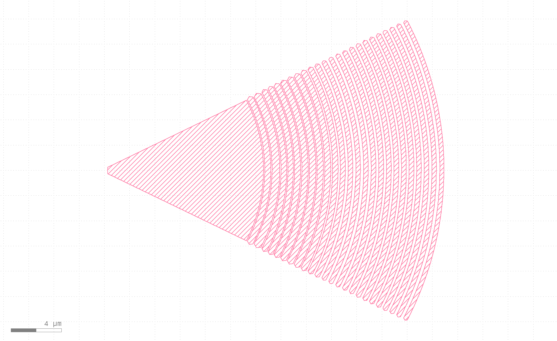
Above is a gds depiction of a grating coupler. Consider a beam of light propogating from the short tapered end of the grating coupler at the left into the grating teeth at the right. When the light interacts with the teeth. The diffraction pattern and interference will result in a propogating wave, orthogonal to the array of grating teeth. You might imagine holding a fiber optic cable up to the grating coupler as if to “catch” the light.
In order to visualize the Bragg diffraction at work here, consider the 2d simulation of a cross-section of the center of the waveguide given below:
import meep as mp
from meep.materials import SiO2
import numpy as np
import matplotlib.pyplot as plt

geometry = []
cell_x = 30
cell_y = 25
cell = mp.Vector3(cell_x, cell_y, 0)
x_offset = cell_x / 2

# Geometry parameters in nanometers
num_teeth = 30
waveguide_depth = .220
etch_depth = 0.068
grating_period = 0.659
fill_factor = 0.524

# Define materials
Si = mp.Medium(index=3.45)
SiO2 = mp.Medium(index=1.45)

# Define wavelength in um
wvl = 1.55

# Construct the geometries
mp.verbosity(level=0)


waveguide = [mp.Block(mp.Vector3(mp.inf,waveguide_depth,mp.inf),
                     center=mp.Vector3(),
                     material=mp.Medium(epsilon=12),  # instead of epsilon, you can use index for defining the index of refraction
                     )]

cladding_depth = 0.5
cladding = [mp.Block(mp.Vector3(mp.inf, cladding_depth, mp.inf),
                 center=mp.Vector3(0, waveguide_depth / 2 + cladding_depth / 2),
                 material=mp.Medium(epsilon=SiO2.epsilon(1 / 1.55)[0][0])
                 )]

box_depth = 2
box = [mp.Block(mp.Vector3(mp.inf, box_depth, mp.inf),
                 center=mp.Vector3(0, -waveguide_depth / 2 - box_depth / 2),
                 material=mp.Medium(epsilon=SiO2.epsilon(1 / 1.55)[0][0])
                 )]

substrate_depth = 700
substrate = [mp.Block(mp.Vector3(mp.inf, substrate_depth, mp.inf),
                 center=mp.Vector3(0, -waveguide_depth / 2 - box_depth - substrate_depth / 2),
                 material=mp.Medium(epsilon=12)
                 )]

etches = []

for i in range(num_teeth):
    etches += [mp.Block(mp.Vector3(grating_period-fill_factor, etch_depth,mp.inf),
                        center=mp.Vector3(i * grating_period + cell_x / 3 - x_offset, (waveguide_depth / 2) - etch_depth/2),
                        material=mp.Medium(epsilon=SiO2.epsilon(1 / 1.55)[0][0]),
                        )]


geometry += cladding
geometry += waveguide
geometry += box
geometry += substrate
geometry += etches

fcen = 1 / 1.55  # pulse center frequency
df = 0.2     # pulse width (in frequency)

sources = [mp.Source(mp.GaussianSource(fcen,fwidth=df),
                     component=mp.Ez,
                     center=mp.Vector3(2 - x_offset,0,0),
                     size=mp.Vector3(0,waveguide_depth,0))]

pml_layers = [mp.PML(1.0)]

resolution = 500

sim = mp.Simulation(cell_size=cell,
                    boundary_layers=pml_layers,
                    geometry=geometry,
                    sources=sources,
                    resolution=resolution)

sim.plot2D()
plt.savefig('grating_coupler_plot.png')
from PIL import Image
import glob
import os

# Capture electric field intensity over time and output into a gif
sim.run(mp.at_beginning(mp.output_epsilon),
        mp.to_appended("ez", mp.at_every(2, mp.output_efield_z)),
        until=200)

# Generate pngs from the simulation output
# This line assumes that colormaps are working,
# you are in the same directory as the output files,
# and that h5py is installed
# If you have a problem with h5utils, see note below
os.system("h5topng -t 0:99 -R -Zc RdBu -A eps-000000.00.h5 -a gray ez.h5")

# Create a gif from the pngs
frames = []
imgs = glob.glob("ez.t*")
imgs.sort()
for i in imgs:
    new_frame = Image.open(i)
    frames.append(new_frame)

# Save into a GIF file that loops forever
frames[0].save('ez.gif', format='GIF',
               append_images=frames[1:],
               save_all=True,
               loop=0)

# Clean up workspace by deleting all generated images
for i in imgs:
    os.remove(i)
Note on h5utils: Sometimes the colormaps in h5utils are invalid when used with Meep. To circumvent this issue, specify the path to your desired colormap using:
(path to h5utils)/h5utils/share/h5utils/colormaps/(desired colormap)
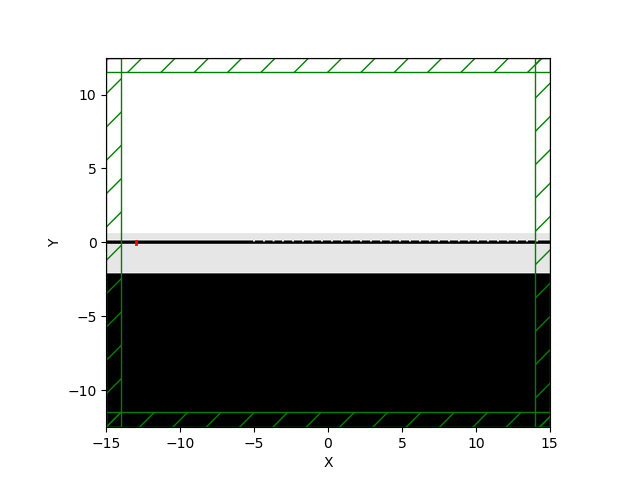
Image of the simulation set-up:
Gif from the meep simulation:
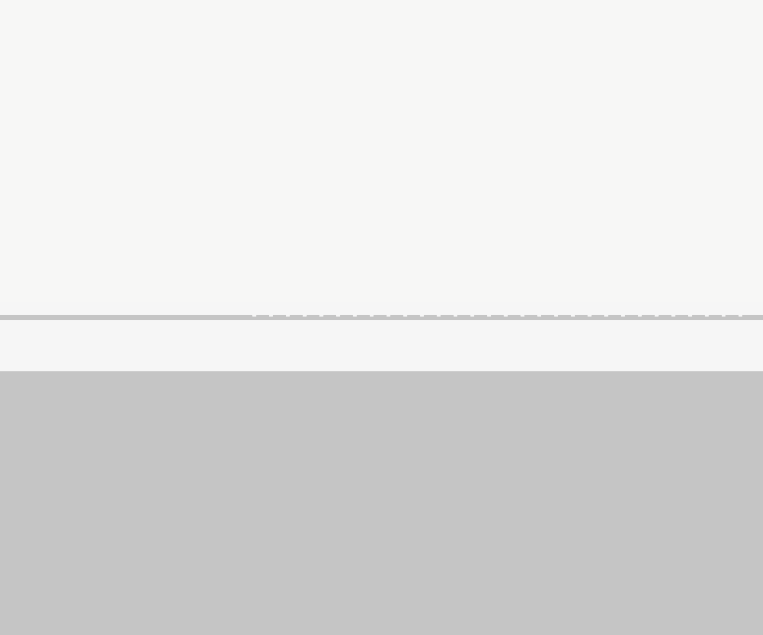
As the light travels, it encounters the periodic grating from the coupler. The diffraction pattern at each of the…
Essential parameters#
It is important to recognize that grating couplers are sensitive to a variety of parameters, some of which will not be discussed in detail in this page. The above demonstration has been optimized for light at 1550 nm, and a 220 nm silicon waveguide. To determine the appropriate parameters for your specific designs, see the analysis page. The following three parameters are essential to a basic understanding of functioning and design of grating coupler.
Simplified cross-sectional view of a grating coupler:
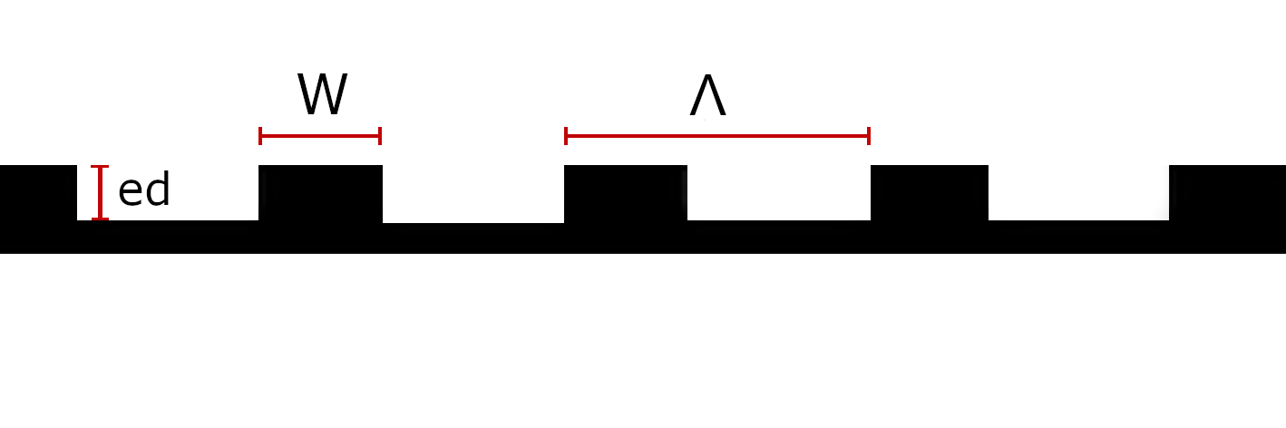
Grating period#
The grating period (typically denoted by \(\Lambda\)) is the parameter most likely to effect the efficiency of a grating coupler. It is the length of one period of the grating, and is measured in microns. The grating period is related to the output angle of the light by the following equation, known as the Bragg condition:
\( \frac{\lambda}{\Lambda} = n_{eff} - \sin(\theta_{air}) \)
where \(\lambda\) is the free-space wavelength of the light, \(n_{eff}\) is the effective index of the grating, and \(\theta_{air}\) is the angle of propogation of the light in the air compared to the surface normal.
Warning
If we were choose the grating period such that the light would be diffracted at exactly 90 degrees, a byproduct of this diffraction would be a large amount of light reflected back into the waveguide. This is because there are different grating orders. The bragg equation above gives us the angle of the first order diffraction, but the second order will indcue twice the amount of change in direction. In the case of a waveguide, light would be reflected back along the waveguide. To avoid this, the grating period is typically chosen to result in a diffraction angle slightly less than 90 degrees, which is ideal for coupling light into a fiber optic cable.
Grating etch depth#
The grating etch depth is the depth of the grating teeth into the silicon waveguide. As the etch depth increases, the effective index of refraction of the etched area also decreases. The overall effective index of refraction of the grating coupler is a weighted average of the effective index of the etched and unetched areas.
Grating fill factor#
The grating fill factor is the ratio of the width of the grating teeth to the width of the grating period. The fill factor will affect the effective index of the grating.
\( ff = \frac{w}{\Lambda} \)
Sources#
“Silicon Photonics Design” by Lukas Chrostowski